
15 Sep 2017
(Via Nanotechweb and UCM) A new work published in the journal Nature Nanotechnology could be the basis to create faster and smaller electronic devices. The research has been carried out by researchers from the Materials Physics department of the UCM and the Institute of Materials Science of Madrid (ICMM-CSIC), users of RES resources,
With the aim of keeping on with the fast pace of increase in storage capacity and computer speed (characterized by the so-called “Moore’s Law”), scientist are now looking for alternatives to conventional electronics based on semiconductors such as silicon. Thanks to the progress of nanotechnology, the production of devices as small as few nanometers is becoming easier and offers the possibility to explore quantum physical phenomena that have been inaccessible until now.
Among these alternatives, there is the use of “domain walls” in ferromagnetic materials. Ferroelectric materials have a permanent dipole moment, or polarization, just like their ferromagnetic counterparts. However, in ferroelectrics, the dipole moment is electric rather than magnetic and can so be oriented using electric fields rather than magnetic ones. The domain walls in ferroelectrics are also much more conducting than the surrounding bulk material and these walls can be moved and erased on demand. This means that they can be used as flexible interfaces with novel functional properties.
Until now, researchers have mainly studied domain-wall conductance for electric current flowing along a wall. Studying the electric conductance across it has proved much more difficult because of the insulating properties of the surrounding material.
A completely new way to design memory devices
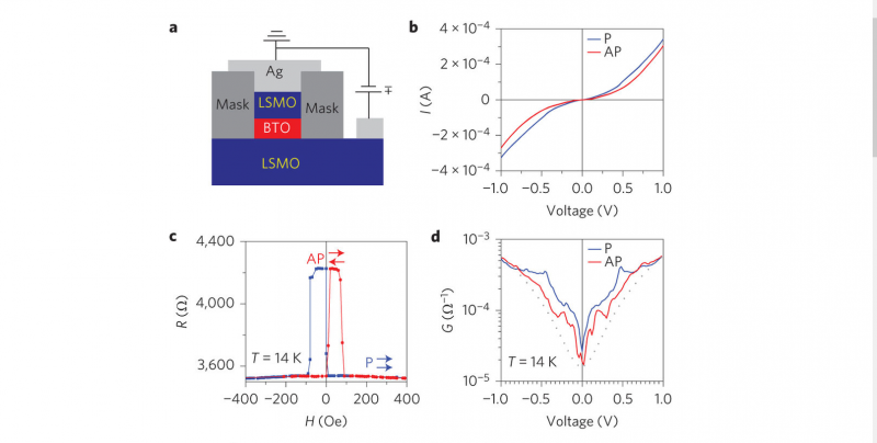
A team led by Jacobo Santamaria, who is at the Universidad Complutense de Madrid and the ICMM-CSIC, also in Madrid, has overcome this challenge. The researchers looked at how electrons travel across a ferroelectric domain wall in a multiferroic tunnel junction based on ferromagnetic La0.7Sr0.3MnO3 electrodes separated by an ultrathin ferroelectric BaTiO3 tunnel barrier. They grew their samples using a sputter deposition technique in pure oxygen plasma at temperatures of 900°C. “This technique determines the interface polarity (atomic plane terminations at the interface between the two materials), which is essential for stabilizing the domain wall,” explains Santamaria. “We confirmed the presence of the domain wall by atomic resolution microscopy and made magnetic tunnel junctions from our samples using optical lithography.”
Juan Ignacio Beltran, from UCM, has been in charge of the computing tasks of this project with the objective to compute from first principles the relevant factors governing the structural and electronic mechanisms that cannot be disentangled by the measurements. This calculations have been performed in Magerit supercomputer, through the Spanish Supercomputing Network (RES) calls.
Integrating domain walls in ferroelectric barriers provides us with a completely new way to design memory devices in which the resistance of the memory can be controlled, not by the ferroelectric polarization (as has been demonstrated in previous studies) but by a single ferroelectric domain wall. This could allow for unprecedented tunability of electron transport in such memories. There is still much to do though before such devices see the light of day, admits Santamaria. “Although we have shown that we can erase the domain walls by switching the ferroelectric polarization, we have yet been unable to stabilize them again (after erasing). Our future efforts will focus on ‘writing’ the domain walls by applying sequences of electric pulses.”
Reference
Sanchez-Santolino, G., Tornos, J., Hernandez-Martin, D., Beltran, J.I., Munuera, C., Cabero, M., Perez-Muñoz, A., Ricote, J., Mompean, F., Garcia-Hernandez, M. and Sefrioui, Z., 2017. Resonant electron tunnelling assisted by charged domain walls in multiferroic tunnel junctions. Nature Nanotechnology. doi:10.1038/nnano.2017.51.

